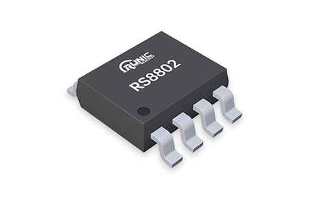
Run-Ic New product release – RS8802
Run-IC are glad to announce the release of Low side Gate Driver RS8802.
Target application: Switching Power Supply/DC-DC Switching Power/Motor Control/Solar Power/UPS/White goods……
Cross reference:
RS8802: ADP3654(ADI) UCC27524A (TI)
RS8802: Single-Channel High-Speed Low-Side Gate Driver with Negative Input Voltage Capability (with 5A Peak Source and Sink)
1 FEATURES
- Low-Cost Gate-Driver Device Offering Superior Replacement of NPN and PNP Discrete Solutions
- 5A Peak-Source and Sink Symmetrical Drive
- Ability to Handle Negative Voltages (-4V) at Inputs
- Fast Propagation Delays (11ns typical)
- Fast Rise and Fall Times (8.5ns and 7ns typical)
- 4.5V to 18V Single-Supply Range
- Outputs Held Low During VDD UVLO (ensures glitch-free operation at power up and power down)
- TTL and CMOS Compatible Input-Logic Threshold (independent of supply voltage)
- Hysteretic-Logic Thresholds for High-Noise Immunity
- Dual Input Design (choice of an inverting (INpin) or non-inverting (IN+ pin) driver configuration) – Unused
- Input Pin can be Used for Enable or Disable Function
- Output Held Low when Input Pins are Floating
- Input Pin Absolute Maximum Voltage Levels Not Restricted by VDD Pin Bias Supply Voltage
- Operating Temperature Range of –40°C to +140°C
- Micro SIZE PACKAGES: SOT23-5
2 APPLICATIONS
- Switch-Mode Power Supplies
- DC-to-DC Converters
- Companion Gate-Driver Devices for DigitalPower Controllers
- Solar Power, Motor Control, UPS
- Gate Driver for Emerging Wide Band-Gap Power Devices (such as GaN)
3 DESCRIPTIONS
The RS8802 dual-channel, high-speed, low-side gate driver device is capable of effectively driving MOSFET
and IGBT power switches. Using a design that inherently minimizes shoot-through current, the RS8802 is capable of sourcing and sinking high peak current pulses into capacitive loads offering rail-to-rail drive capability and extremely small propagation delay typically 13ns.
The RS8802 device is capable of handling -4V at input. In addition, the drivers feature matched internal propagation delays between the two channels, these delays are very well suited for applications requiring dual-gate drives with critical timing, such as synchronous rectifiers. This also enables connecting two channels in parallel to effectively increase currentdrive capability or driving two switches in parallel with one input signal.
The RS8802 provides 5A source and 5A sink (symmetrical drive) peak-drive current capability at VDD = 12V.
The RS8802 is designed to operate over a wide VDD range of 4.5 V to 18 V and wide temperature range of -40°C to 140°C. Internal Undervoltage Lockout (UVLO) circuitry on VDD pin holds output low outside VDD operating range. The capability to operate at low voltage levels such as below 5V, along with best-inclass switching characteristics, is especially suited for driving emerging wide band-gap power-switching devices as GaN power semiconductor devices.